「硅光之父」Richard Soref再发Chip!硅基超晶格-绝缘体集成电路中电场诱导的准相位匹配三波混合
FUTURE远见| 2023-06-28
Future|远见
Future|远见future选编
超晶格-绝缘体晶圆,例如300毫米的硅-绝缘体晶圆,目前是一个在多个光电领域具有高性能应用前景的理论构想²。该种由晶片键合制成的异质集成晶圆可以被进一步切割,从而提供具有独特性能的光子或光电集成芯片。理论分析已经指出,上述光子/光电集成芯片具有强的泡克尔斯效应(Pockels effect),显著的非线性光学性质,以及显著的电场诱导的三波混合(electric-field-induced three-wave mixing, EFIM)。本工作即着重结合物理理论和工程学考虑,研究基于(ZnS)៷/(Si₂)៳短周期超晶格-绝缘体材料的光学波导和集成赛道谐振器等集成光子器件(图1)的EFIM性质。
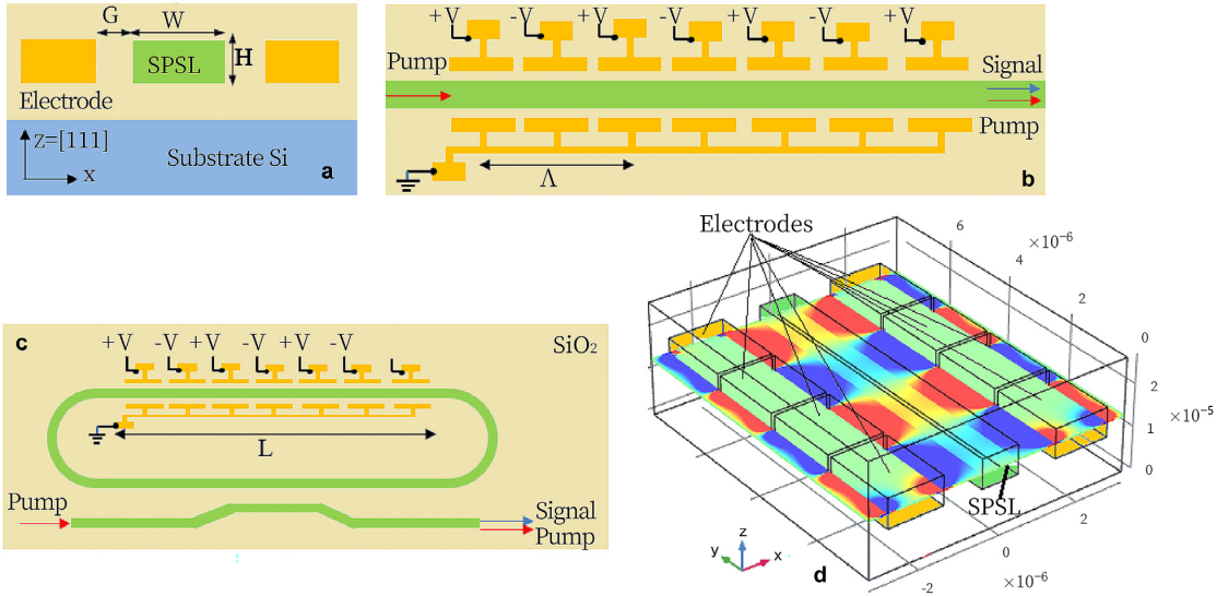
图1 | 展现EFIM过程的集成光子器件示意图。a,本工作提出的SiO₂包层的ZnS/Si短周期超晶格(short-period superlattice, SPSL)条形波导截面图。b,具有SPSL条形波导的EFIM器件的顶上观以及具有准相位匹配的周期性反向施加电压(periodically reversed applied voltage,PRAV)电极的周期性空间分布。c,作为展示共振EFIM过程平台的母线耦合赛道腔体的顶上观。d,周期性空间排布PRAV电极产生直流电场的三维模拟。
研究者基于紧束缚哈密顿的理论研究提出了在一个无掺杂短周期超晶格中的显著EFIM,而该EFIM过程则被体现于集成于光电芯片上的准相位匹配的(quasi-phase matching, QPM)超晶格垂直波导和超晶格赛道谐振器。三阶非线性光学敏感度()和线性磁化率的光谱被模拟为「非松弛」异质界面原子单层数量的函数,并考虑了价带和导带之间的所有跃迁。较大的
值使得(ZnS)₃/(Si₂)₃ SPSL成为实现大的有效二阶非线性的良好候选材料,从而使得基于超晶格-绝缘体结构的光子和光电集成线路有望在1000 nm和2000 nm波长范围内实现高性能。研究者对二次谐波产生(second harmonic generation, SHG)的效率(图2)和光参量振荡器(optical parametric oscillator, OPO)的性能(图3)进行了详细的计算。结果表明,(ZnS)៷/(Si₂)៳ QPM与现有的周期性极化的铌酸锂(periodically poled lithium niobate, PPLN)光子学平台技术相比具有竞争力,在经典和量子应用方面具有实用性。
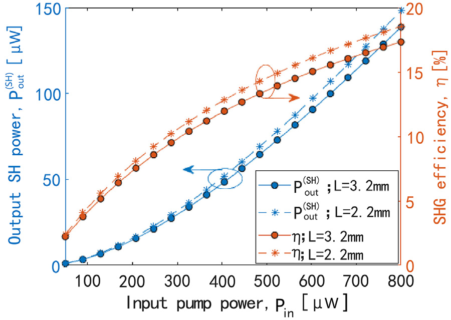
图2 | 二阶谐波输出功率和转换效率随输入泵功率的变化,对比于不同的QPM段长度值。
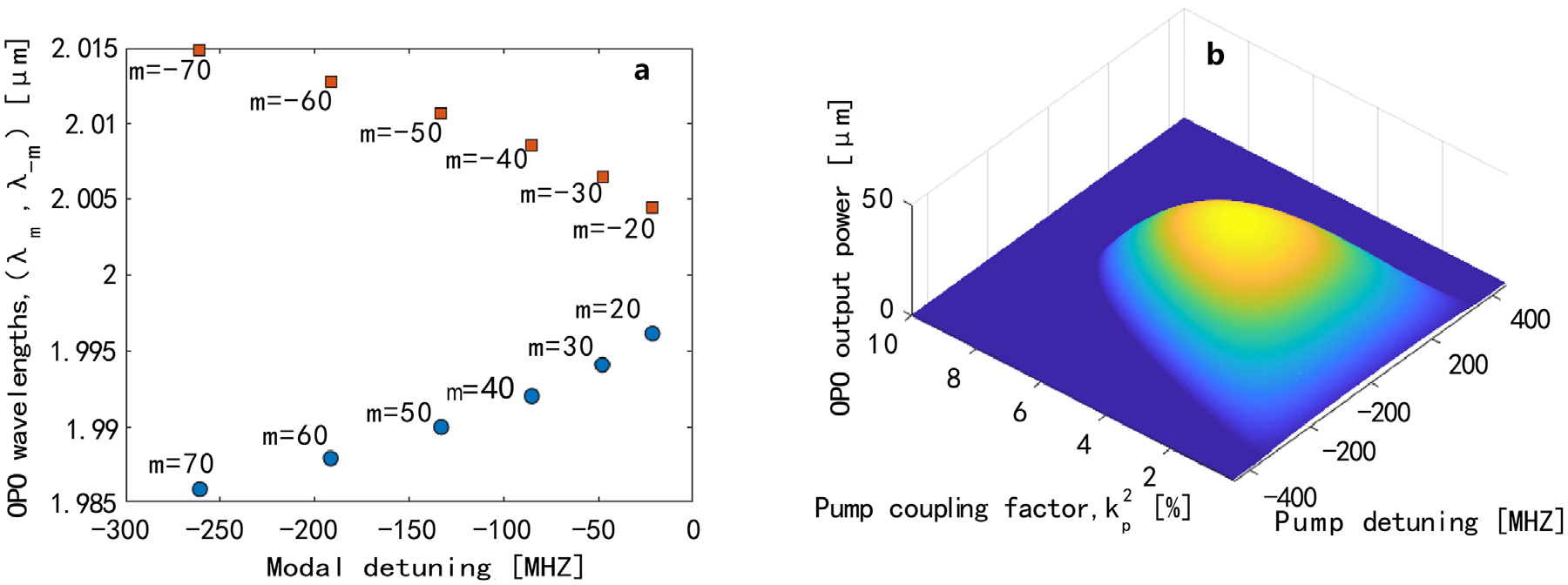
图3 | a,OPO振荡波长与模态失谐的关系。b,非简并OPO输出功率随泵浦失谐和泵浦耦合因子的变化。
在光子学文献中有大量电场诱导和极化诱导的χ⁽²⁾ 效应的现有技术,而实现这些效应的材料包括Si、SiO₂、Si₃N₄、玻璃纤维、聚合物、BaTiO₃和LiNbO₃³⁻⁷。然而,多年来,PPLN一直是QPM频率转换公认的领先者。在本工作中,研究者对超晶格PRAV和目前的PPLN技术进行了比较,并得出结论:对于SHG和OPO,「具有代表性的」ZnS/Si堆叠超晶格的性能与PPLN的性能相当,或ZnS/Si堆叠超晶格更具有竞争性。值得强调的是,这个工作为超晶格波导中的分层接近理想状况时的预期性能提供了理论指导。当然,在实际实验中会有制造的误差,包括表面粗糙度、蚀刻误差、层厚变化、点缺陷、螺位错,以及不如人意的应力、意外的掺杂。这些误差会在无源SLOI波导内引起传播损耗,并会降低SLOI EFIM器件的性能指标。
综上,利用(ZnS)₃/(Si₂)₃超晶格提供的大电场诱导的值,本工作从理论上预测,上述材料的片上共振SHG和OPO的性能可与LNOI平台的实验结果相媲美。因此,本工作为(ZnS)៷/(Si₂)៳超晶格平台在未来用于具有经典和量子应用的实验性异质SLOI光电/光子芯片提供了理论依据。
Electric-field-induced quasi-phase-matched three-wave mixing in silicon-based superlattice-on-insulator integrated circuits¹
The superlattice-on-insulator wafer–, such as the 300-mm silicon wafer–, is presently a theoretical-physics vision that promises high performance in several opto-electronics areas². Formed by wafer bonding, this heterogeneously integrated wafer would be diced into chips offering uniquely capable photonic and opto-electronic integrated circuits (PICs and OEICs). Our theoretical analysis indicates that the chips will have strong Pockels effect, large optical nonlinearities, and large electric-field-induced three-wave mixing, EFIM, which is the topic of this paper.
Researchers present a theoretical investigation, based on the tight-binding Hamiltonian, of efficient electric-field-induced three-waves mixing (EFIM) in an undoped lattice-matched short-period superlattice (SL) that integrates quasi-phase-matched (QPM) SL straight waveguides and SL racetrack resonators on an opto-electronic chip. Periodically reversed DC voltage is applied to electrode segments on each side of the strip waveguide. The spectra of and of the linear susceptibility have been simulated as a function of the number of the atomic monolayers for 「non-relaxed」 heterointerfaces, and by considering all the transitions between valence and conduction bands. The large obtained values of
make the (ZnS)₃/(Si₂)₃ short-period SL a good candidate for realizing large effective second-order nonlinearity, enabling future high-performance of the SLOI PICs and OEICs in the 1000-nm and 2000-nm wavelengths ranges. Researchers have made detailed calculations of the efficiency of second-harmonic generation and of the performances of the optical parametric oscillator (OPO). The results indicate that the (ZnS)៷/(Si₂)៳ QPM is competitive with present PPLN technologies and is practical for classical and quantum applications.
There is considerable prior art in the photonics literature on E-field-induced and poling-induced χ⁽²⁾ effects in Si, SiO₂, Si₃N₄, glass fiber, polymer, BaTiO₃ and LiNbO₃ ³⁻⁷. However, for years, the periodically poled lithium niobate photonics platform, PPLN, has been the acknowledged leader in QPM frequency conversion. In the studies given here, researchers make comparisons of the SL PRAV to the present PPLN art, and researchers conclude that superlattice performance for the 「representative」 ZnS/Si stack will be comparable to, or competitive with, the PPLN performance in SHG and OPO. It is worth repeating that the work here provides theoretical guidelines on performance expected if the layering within superlattice waveguides is nearly perfect. Of course, in developmental experiments, there will be fabrication errors including surface roughness, etching errors, variation in layer thicknesses, point defects, threading dislocations and perhaps unwanted strain as well as unintentional doping. Such errors will induce propagation loss within the passive SLOI waveguides and will decrease the performance metrics for the SLOI EFIM devices.
Using the large electric-field-induced values provided by (ZnS)₃/(Si₂)₃ superlattices, researchers predict on-chip resonant SHG and OPO with performances comparable to the results experimentally found for the LNOI platform. For the above reasons, the present work offers a performance motivation for using the (ZnS)៷/(Si₂)៳ SL platform in future experimental heterogeneous SLOI opto-electronc PIC chips for classical and quantum applications.
作者信息
Richard A. Soref毕业于美国斯坦福大学。现任美国马萨诸塞大学波士顿分校工程学院研究教授,电子电气工程师学会终身会士(IEEE Life Fellow),Optica(前美国光学会,OSA)会士,2019年国际工程与技术学会(IET)终身成就奖章(Achievement Medal)获得者。在其迄今长达近60年的科研生涯中,Soref教授对硅基光子学领域做出过奠基性、突出性贡献,以「硅光之父」著称。至今,Soref教授已累计发表研究论文约600篇,并著有11个专著章节,拥有54项美国专利。谷歌学术显示Soref教授著作至今已累计被引用31000余次,h指数84。
Francesco De Leonardis毕业于意大利巴里理工大学,自2018年起担任巴里理工大学电子与信息工程系副教授。De Leonardis教授同时担任意大利国家核物理所副研究员以及光子纳米技术所副研究员。至今De Leonardis教授已累计发表超过150篇研究论文,并持有1项国际专利。谷歌学术显示De Leonardis教授至今已累计被引2300余次,h指数25。
参考文献:
1. Soref, R. & De Leonardis, F. Electric-field-induced quasi-phase-matched three-wave mixing in silicon-based superlattice-on-insulator integrated circuits. Chip 2, 100042 (2023).
2. Soref, R., Shastri, B. J. & Tait, A. N. The silicon-based XOI wafer: the most general electronics-photonics platform for computing, sensing, and communications. IEEE J. Sel. Top. Quantum Electron. 29, 1–8 (2023).
3. Widhalm, A. et al. Electric-field-induced second harmonic generation in silicon dioxide. Opt. Express 30, 4867–4874 (2022).
4. Zabelich, B., Nitiss, E., Stroganov, A. & Brès, C.-S. Linear electro-optic effect in silicon nitride waveguides enabled by electric-field poling. ACS Photonics 9, 3374–3383 (2022).
5. Chen, S., Li, K. F., Li, G., Cheah, K. W. & Zhang, S. Gigantic electric-field- induced second harmonic generation from an organic conjugated polymer enhanced by a band-edge effect. Light. Sci. Appl. 8, 17 (2019).
6. Li, Z., Yuan, B., Wang, S., Wang, M. & Bing, P. Periodically poled BaTiO₃: an excellent crystal for terahertz wave generation by cascaded difference frequency generation. Curr. Opt. Photon. 2, 179–184 (2018).
7. Rao, A. et al. Second harmonic generation in periodically poled thin film lithium niobate wafer bonded on silicon. Opt. Express 24, 29941–29947 (2016).
论文链接:
https://www.sciencedirect.com/science/article/pii/S2709472323000059
关于Chip
Chip是全球唯一聚焦芯片类研究的综合性国际期刊,已入选由中国科协、教育部、科技部、中科院等单位联合实施的「中国科技期刊卓越行动计划高起点新刊项目」,为科技部鼓励发表「三类高质量论文」期刊之一。
Chip期刊由上海交通大学与Elsevier集团合作出版,并与多家国内外知名学术组织展开合作,为学术会议提供高质量交流平台。
Chip秉承创刊理念: All About Chip,聚焦芯片,兼容并包,旨在发表与芯片相关的各科研领域尖端突破性成果,助力未来芯片科技发展。迄今为止,Chip已在其编委会汇集了来自14个国家的70名世界知名专家学者,其中包括多名中外院士及IEEE、ACM、Optica等知名国际学会终身会士(Fellow)。
Chip第二卷第二期(2023年夏刊)即将于2023年6月在爱思维尔Chip官网以金色开放获取形式(Gold Open Access)发布,欢迎访问阅读本期最新文章。
爱思唯尔Chip官网:
https://www.journals.elsevier.com/chip