Chip发表东北大学王军团队最新成果:基于0D-2D钙钛矿异质结构的高性能柔性光电探测器
FUTURE远见| 2023-03-14
Future|远见
Future|远见future选编

柔性光电探测器是可穿戴设备、可折叠显示器件、生物医学成像等系统中至关重要的有源器件。得益于高光学吸收系数、高载流子迁移率、可调节带隙等特性,有机-无机杂化钙钛矿材料在柔性光电器件中的应用已经有不少报道,但是,先前报道的此类器件大多数是基于单一维度的钙钛矿材料。近年来,基于异质结结构的光电探测器在现代纳米技术的各类应用领域中展示了巨大的潜力,包括视频成像、夜视、光通信、运动监测等。使用异质结钙钛矿材料有望进一步提高器件的性能。
因此,本研究基于二维Dion-Jacobson (2D DJ)钙钛矿(4AMP)(MA)₂Pb₃I₁₀(n3)和微浓度CsPbI₃QDs(QDs)设计了n3/QDs层状异质结构的柔性紫外-近红外光电探测器。QDs显示出强烈的光敏性和高功率输出,在660 nm光下最佳浓度QDs的器件响应度增加到615%。两者的带隙接近,形成能带匹配的结构,降低了载流子传输势垒。QDs层填充钙钛矿膜的间隙,形成良好的异质结构。QDs层隔离水并钝化钙钛矿层,以实现光电子器件的高稳定性能。在高达5000次弯曲形变和不同弯曲角度下,具有最佳QD浓度的光电探测器的性能几乎保持不变,并且随着弯曲循环次数的增加,器件表现出自愈现象。本工作的研究将为柔性可穿戴技术的发展、构建高性能低成本的光电探测器提供一种新的思路。
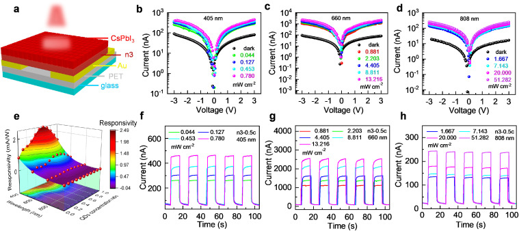
n3/QDs层状异质结构光电探测器是通过在n3薄膜上旋涂不同浓度的QDs制备而成。通过优化QDs浓度以获得最佳光电性能。与其他光照相比,所有器件在660 nm光照下具有最佳的光响应。这是光源能量与带隙匹配的结果(n3:1.99 eV,QD:1.80 eV)。在660 nm光照下,n3-0.5c的光电流比n3大515%。(图1)
在3 V偏压660 nm光照下,柔性n3-0.5c器件在不同弯曲次数后其暗电流和光电流都略比未弯曲前的低。经5000次弯曲形变后器件的光响应仍能保持初始状态的97%。当弯曲的半径从6.08 mm增加至11.36 mm时,n3-0.5c器件的光电流不发生变化。整体来说,n3-0.5c光电探测器具有良好的机械柔韧性。(图2)
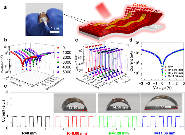 图2 | n3/QDs层状异质结构光电探测器件应力相应研究。
由于n3和QD的导带底(CBM)和价带顶(VBM)之间的差异非常小,载流子传输过程能量势垒匹配。n3-0.5c异质结构具有最长寿命。带隙较大的钙钛矿产生的光电子和空穴成为激子。量子点提高了钙钛矿中的载流子传输效率,并发出带隙更窄的明亮光²。在光照下,作为光敏层的量子点吸收入射光以生成电子-空穴对。电子和空穴被转移到Au电极上从而产生光电流。通过调节异质结结构中的量子点浓度可以获得最佳的光电性能。(图3)
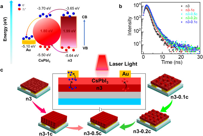 图3 | 光电探测器可能的机理示意图。
值得一提的是,这种基于0D/2D钙钛矿异质结结构的光电探测器件可通过旋涂等方法制备而成,其制备工艺简单和制备成本低廉,研制出的高性能柔性钙钛矿光电探测器有望集成于可穿戴设备和其它柔性光电子器件中,比如人造眼、柔性智能手机等等。
High performance flexible photodetector based on 0D-2D perovskite heterostructure¹
A flexible Vis-NIR photodetector (PD) is designed containing two-dimensional Dion-Jacobson (2D DJ) perovskite (4AMP)(MA)₂Pb₃I₁₀ (n3) and the micro concentration of CsPbI₃ perovskite quantum dots (QDs) layered heterostructures. QDs depict strong photosensitivity and high-power output, and the device response under 660 nm light is increased to 615% controlled by the optimal concentration of QDs. The degradation of PDs with the optimal concentration of QDs under up to 5000 bending cycles and different bending angles can be ignored, and the devices show a self-healing phenomenon with the increase of bending cycles. The optimized strategy will develop flexible, wearable, high-performance, and low-cost PDs.
The device is fabricated with different concentrations of QDs by spin coating onto the n3 thin film. QDs concentration is optimized for the optimum photoelectric performance. The data obtained for all devices in the horizontal aspect has the best photoresponse at 660 nm when compared to the other laser lights. This is the result of energy drawn from a light source matching the band gap (n3: 1.99 eV, QDs: 1.80 eV). From vertical dimension, the photocurrent of n3-0.5c is by 515% more than n3 under 660 nm. (Fig. 1)
Flexibility of n3-0.5c PD having the flattest thin film is measured by I-V logarithm curves and I-t curves as the function of bending cycle numbers under 660 nm light illumination at 3 V bias (Intensity: 4.405 mW cm⁻²). The dark and light currents slightly decrease compared to their initial values. 97% photo-response is intact up to 5000 bending cycles. The n3-0.5c device can withstand bending of various radii from 6.08 mm to 11.36 mm. The device photocurrent is not changing as the bending degree increases. The results reveal excellent mechanical flexibility of n3-0.5c PD. (Fig. 2)
The difference between CBM and VBM of the n3 and QDs is very small, forming a band-matching structure that lowers the energy barrier of carrier transport process. The n3-0.5c heterostructure has the longest lifetime. Photoelectrons and holes generated from perovskite with larger band gaps become excitons. The presence of quantum dots improves efficiency through carrier transportation in perovskite and emits bright light with a narrower band gap⁴. Under the light, QDs as photosensitive layers absorb incident light for generating electron-hole pairs. The electrons and holes are transferred to Au electrode for producing photocurrent. The best photoelectric performance is obtained by adjusting the QDs concentration in the heterojunction structure (Fig. 3).
参考文献:
1. Ma, Y., Li, Y., Wang, H., Wang, M. & Wang, J. High performance flexible photodetector based on 0D-2D perovskite heterostructure. Chip 2, 100032 (2022).
2. Ning, Z. et al. Quantum-dot-in-perovskite solids. Nature 523, 324-328 (2015).
论文链接:
https://www.sciencedirect.com/science/article/pii/S2709472322000302
关于Chip
Chip是全球唯一聚焦芯片类研究的综合性国际期刊,已入选由中国科协、教育部、科技部、中科院等单位联合实施的「中国科技期刊卓越行动计划高起点新刊项目」,为科技部鼓励发表「三类高质量论文」期刊之一。
Chip期刊由上海交通大学与Elsevier集团合作出版,并与多家国内外知名学术组织展开合作,为学术会议提供高质量交流平台。
Chip秉承创刊理念: All About Chip,聚焦芯片,兼容并包,旨在发表与芯片相关的各科研领域尖端突破性成果,助力未来芯片科技发展。迄今为止,Chip已在其编委会汇集了来自14个国家的70名世界知名专家学者,其中包括多名中外院士及IEEE、ACM、Optica等知名国际学会终身会士(Fellow)。
Chip第二卷第一期(2023年春季刊)于2023年03月在爱思唯尔Chip官网以金色开放获取形式(Gold Open Access)发布,欢迎访问阅读文章。
爱思唯尔Chip官网:
https://www.journals.elsevier.com/chip