Chip发表佐治亚理工大学Suman Datta教授团队最新成果:用于高性能计算的低温CMOS芯片
FUTURE远见| 2024-05-24
Future|远见
Future|远见future选编
近日,佐治亚理工大学Suman Datta教授团队以「The future is frozen: cryogenic CMOS for high-performance computing」¹为题在Chip上发表研究论文,利用实验校准数据来调整阈值电压,并在器件、电路和系统级别研究了低温 CMOS芯片的功耗性能区域。第一和通讯作者为Rakshith Saligram。本文为特刊(Cryogenic Chips)文章之一,此特刊为Chip发起的首个特刊。Chip是全球唯一聚焦芯片类研究的综合性国际期刊,是入选了国家高起点新刊计划的「三类高质量论文」期刊之一。
在过去十年中,高性能计算(High-Performance-Compute,HPC)范式中的计算需求增长了100倍以上,远远超过了经典摩尔定律中晶体管密度的增长率。跨技术节点的性能增益的历史速率的降低、无法按比例降低的阈值电压、功率密度的增加等都是造成当前情况的原因。数据中心将超过三分之一的电力预算投资于冷却设备,其目的只是防止服务器因过热而停机。当前,冷却系统,特别是浸入式冷却系统,开始应用于超频处理器,而性能的改进仍是微不足道的(约20%)²。低温互补金属氧化物半导体(Complementary Metal Oxide Semiconductor ,CMOS)可在比传统冷却系统更低的温度下工作,从而提供更高的性能³。
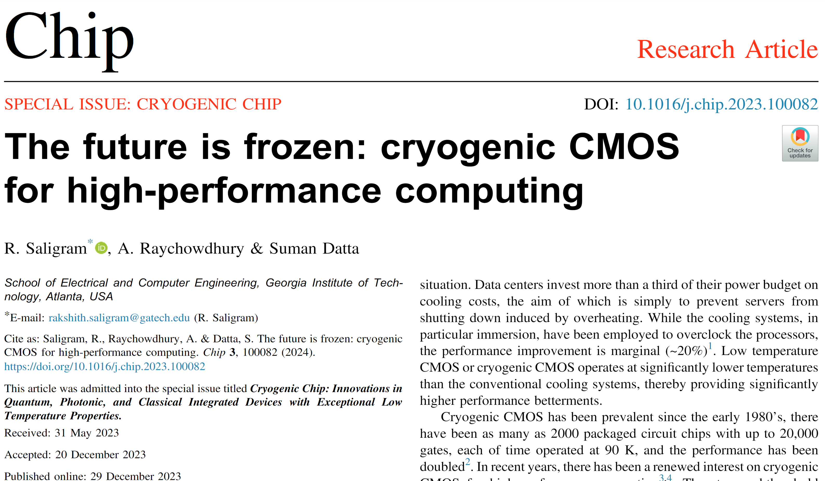
该文中,研究团队提出了用于低温CMOS校准的Berkeley短沟道绝缘栅型场效应管(IGFET)模型(BSIM),该模型使用来自14 nm节点鳍场效应晶体管(Fin Field Effect Transistor,FinFET)的测量数据进行校准。作者还介绍了在低温下工作的在28 nm 体硅CMOS工艺技术和22 nm 全耗尽型绝缘衬底上硅(Fully Depleted Silicon on Insulator, FDSOI )之下制造的功能存储器芯片的测量和分析结果,采用Lakeshore CPX-VF低温探测站从300 K到4 K测量了14 nm节点的FinFET器件(图1)。在四幅图中都确定了一个关键的兴趣点—零温度系数(ZTC)点。该栅极电压/漏极电流在设计具有温度弹性的电路中是关键的,并且栅极电压的大小必须高于器件的ZTC值,以显示器件导通电流的改善。从曲线图中可以看出,器件泄漏电流呈指数级下降,而导通电流却随着温度的降低而线性增加。
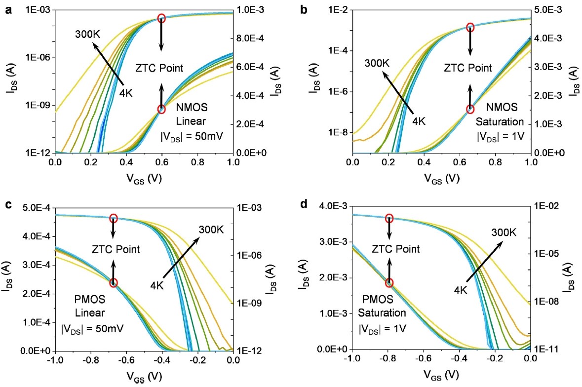
图1 NMOS(a,b)和PMOS(c,d)的线性和饱和区域中的晶体管传输特性,其显示出导通电流的线性增加以及亚阈值漏电流的指数下降。
研究团队提出,可以采用阈值电压(Vₜₕ)工程来调节器件的Vₜₕ,从而增加整个温度的电流增益,获得性能增益。对于给定的栅极过驱动电压,该方法还产生更高的器件电流。团队根据经验进一步调整了模型中的PHIG变量,模拟Vₜₕ调整,以获得iso-IOFF或iso-Vₜₕ场景,从而分析电路和系统等IOFF条件下三个关键低温的归一化电流如图2所示。
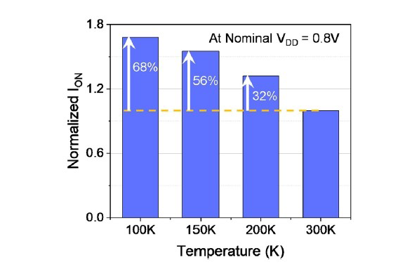
图2 在关键温度点之间的标称电源电压下,器件接通电流的标准化增加。
研究小组采用上述标准单元库,在温度和电源电压范围内采用了Arm Cortex-A53 CPU⁴。他们选择了一个11层金属层后端(Back End of Line,BEOL)堆叠用于设计实现,顶部两层专门用于执行电源和接地布线,而其余层用于信号和电源布线。在0.8 V的标称电源电压下,Cortex-A53内核的性能从300 K提高到100 K,提高了56%(图3)。功率的增加源于(i)时钟频率的增加和(ii)总开关电容(Csw)的增加,Csw的增加又是由于具有较低Vₜₕ器件的输入栅极电容的增加、栅极尺寸的增大以实现更高的目标频率和用于保持固定的更多缓冲。
图3 Cortex-A53内核在不同温度点的标称VDD下的性能基准测试。
综上所述,低温CMOS芯片在高性能计算中具有巨大的应用潜力。这是由器件特性的改善带来的,包括由于更高的载流子迁移率、指数低的漏电流、更陡的亚阈值摆幅(SS)、降低的本征电阻、降低的接触电阻等而增加的导通电流。BEOL互连也得到改进,这要归功于在低温下较低的体电阻率和由于较低的焦耳加热而提高的可靠性。此外,由于泄漏而在室温下不可行的存储器技术,例如伪静态增益单元嵌入式动态随机存取存储器(Embedded Dynamic Random-Access Memory, EDRAM)、浮体随机存取存储器(Random-Access Memory, RAM)等,在低温下是可行的。
低温CMOS芯片的主要优点是,随着温度的降低,性能以可预测的方式从所理解的室温参考点按可预测的形式缩放。低温下的下一个问题是器件了离断电流的可变性增加,正如当前工作中所研究的那样,这种可变性在先进技术节点往往会增加。目前,电路设计技术无法解释这些明显的参数变化,Monte Carlo等统计分析手段会成为设计周期中不可避免的一部分。
The future is frozen: cryogenic CMOS for high-performance computing¹
The compute demand in the high-performance-compute (HPC) paradigm has grown over 100x in the last decade and has well surpassed the rate of growth in transistor density per classical Moore’s law. Reduction in the historical rate of performance gain across technology nodes, the inability to scale down the threshold voltage without increasing the leakage currents, increasing power density forcing throttling of processor clock speed have all contributed to the present situation. Data centers invest more than a third of their power budget on cooling costs, the aim of which is simply to prevent servers from shutting down induced by overheating. While the cooling systems, in particular immersion, have been employed to overclock the processors, the performance improvement is marginal (~20%)². Low temperature complementary metal oxide semiconductor (CMOS) or cryogenic CMOS operates at significantly lower temperatures than the conventional cooling systems, thereby providing significantly higher performance betterments³.
In the current work, the research team presented the Berkeley short-channel IGFET model (BSIM) for cryogenic CMOS calibrated using measurement data from 14 nm node fin field effect transistor (FinFET). The research team also presented results from measurement and analysis of functional memory chips fabricated in 28 nm bulk CMOS and 22 nm fully depleted silicon on insulator (FDSOI) operating at cryogenic temperature (Fig.1). Finally, the challenges and opportunities in the further development and deployment of such systems were discussed.
Fig. 1 | Transistor transfer characteristics in linear and saturation regions for NMOS (a, b) and PMOS (c, d) showing linear increase in ON current, exponential decrease in subthreshold leakage current.
The research group reported that threshold voltage (Vₜₕ) engineering could be employed to tune the Vₜₕ of the devices so as to increase current gain across the temperature, thereby obtaining performance gain. It will also yield higher device current for a given gate overdrive voltage. They further empirically tuned the PHIG variable in the model mimicking the threshold voltage tuning for obtaining iso-IOFF or iso-Vₜₕ scenario to analyze the circuits and systems. The normalized currents for the three key low temperatures under iso-IOFF condition are displayed in Fig. 2.
Fig. 2 | Normalized increase in device ON current at nominal supply voltage across key temperature points.
An Arm Cortex-A53 CPU was across temperatures and supply voltages with the adoption of the aforementioned standard cell libraries⁴. An elevenmetal layer back end of line (BEOL) stack was selected for the design implementation with the top two layers dedicated to performing power and ground routing while the rest were used for both signal and power routing. At a nominal supply voltage of 0.8 V, the performance of the Cortex-A53 core is increased by 56% going from 300 K to 100 K (Fig. 3). The switching power increase stems from (i) increase in clock frequency and (ii) increase in the total switched capacitance (Csw). The Csw increase is in turn from increase in input gate capacitance with lower Vₜₕ devices, up-sizing of gates to achieve higher targeted frequency and more buffering for hold fixing.
Fig. 3 | Normalized increase in device ON current at nominal supply voltage across key temperature points.
To Conclude, cryogenic CMOS has immense potential for applications in high performance computing, which is brought by the improvement in devices characteristics including the increased on current resulted from higher carrier mobility, exponentially low leakage current, steeper subthreshold swing (SS), reduced intrinsic resistances, decreased contact resistance, and so on. The BEOL interconnects show improvement as well, thanks to the lower bulk resistivity at low temperature and improved reliability due to lower joules heating. Furthermore, memory technologies not feasible at room temperature mainly due to leakage, such as pseudo-static gain cell embedded dynamic random-access memory (EDRAM), floating body random-access memory (RAM), and so on, are possible at cryogenic temperature.
The main advantage of low temperature CMOS is that the performance scales in a predictive fashion from the understood room temperature reference points in a predictable manner with decreasing temperature. With ultralow leakage and higher carrier mobility leading to steep SS devices, there is a plethora of opportunities for innovation from material level to devices, circuits design technique and systems which have traditionally been harder to “engineer and optimize” at room temperature. Currently, the circuit design techniques are not enabled to account for these pronounced parameter variation, and statistical analysis like Monte Carlo needs to become an inevitable part of the design cycle.
参考文献:
1. Saligram, R., Raychowdhury, A. & Datta, S. The future is frozen: cryogenic CMOS for high-performance computing. Chip 3, 100082 (2024).
2. Jalili, M. et al. Cost-efficient overclocking in immersion-cooled datacenters. In 2021 ACM/IEEE 48th Annual International Symposium on Computer Architecture (ISCA), 623-636 (IEEE, 2021).
3. Carlson, D. M., Sullivan, D. C., Bach, R. E. & Resnick, D. R. The ETA 10 liquidnitrogen-cooled supercomputer system. IEEE Trans. Electron Devices 36, 1404e1413 (1989).
4. Saligram, R., Prasad, D., Pietromonaco, D., Raychowdhury, A. & Cline, B. A 64-bit arm CPU at cryogenic temperatures: design technology co-optimization for power and performance. In 2021 IEEE Custom Integrated Circuits Conference (CICC), 1-2 (IEEE, 2021).
论文链接:
https://www.sciencedirect.com/science/article/pii/S270947232300045X
作者简介

Suman Datta是佐治亚理工学院电子与计算机工学院教授,佐治亚研究联盟(GRA)杰出学者。Datta教授在美国辛辛那提大学获得博士学位, 他的研究方向为基于全新计算模型的半导体器件,如内存计算、大脑启发计算、低温计算、弹性计算等等。2013年,Datta教授被选为美国电气与电子工程师学会(IEEE)会士。2016年,他荣获美国国家发明家科学院(NAI)院士。
Suman Datta, is the Eminent Scholar and Professor in the School of Electrical & Computer Engineering at Georgia Tech, IEEE Fellow. He has received his Ph.D. degree in Electrical and Computer Engineering from the University of Cincinnati, USA. His research group focuses on semiconductor devices that enable new compute models such as in-memory compute, brain-inspired compute, cryogenic compute, resilient compute etc. In 2013, Datta was named a Fellow of the Institute of Electrical and Electronics Engineers (IEEE). In 2016, he was named Fellow of the National Academy of Inventors (NAI).

Rakshith Saligram是佐治亚理工大学电子与计算机工学院助理研究员,博士毕业于佐治亚理工大学。目前,他的研究专注于低温超大规模集成电路。Saligram在美国南加州大学获得电气工程硕士学位,并在位于加利福尼亚州的Intel公司担任过图形硬件工程师。
Rakshith Saligram, an assistant researcher at the School of Electronic and Computer Engineering at Georgia Tech, with a doctoral degree from the university. Currently, his research focuses on low-temperature ultra large scale integrated circuits. Saligram obtained a Master's degree in Electrical Engineering from the University of Southern California, Los Angeles, and worked as a graphics hardware engineer at Intel in California for over two years.
关于Chip
Chip(ISSN:2772-2724,CN:31-2189/O4)是全球唯一聚焦芯片类研究的综合性国际期刊,已入选由中国科协、教育部、科技部、中科院等单位联合实施的「中国科技期刊卓越行动计划高起点新刊项目」,为科技部鼓励发表「三类高质量论文」期刊之一。
Chip期刊由上海交通大学出版,联合Elsevier集团全球发行,并与多家国内外知名学术组织展开合作,为学术会议提供高质量交流平台。
Chip秉承创刊理念: All About Chip,聚焦芯片,兼容并包,旨在发表与芯片相关的各科研领域尖端突破性成果,助力未来芯片科技发展。迄今为止,Chip已在其编委会汇集了来自14个国家的69名世界知名专家学者,其中包括多名中外院士及IEEE、ACM、Optica等知名国际学会终身会士(Fellow)。
Chip第三卷第一期已于2024年3月在爱思维尔Chip官网以金色开放获取形式(Gold Open Access)发布,欢迎访问阅读本期最新文章。
爱思唯尔Chip官网:
https://www.sciencedirect.com/journal/chip