Chip发表南京大学陈鹏、张荣团队最新成果:具有双势垒阳极结构的横向AIGaN/GaN肖特基势垒二极管
FUTURE远见| 2024-03-14
Future|远见
Future|远见future选编
近日,南京大学陈鹏、张荣团队以「A Lateral AlGaN/GaN Schottky barrier diode with 0.36 V turn-on voltage and 10 kV breakdown voltage by using double barrier anode structure」¹为题在Chip上发表研究论文,采用双势垒阳极结构同时实现0.36V导通电压和10kV击穿电压的AlGaN/GaN肖特基势垒二极管。第一作者为徐儒,通讯作者为陈鹏、张荣和郑有炓。Chip是全球唯一聚焦芯片类研究的综合性国际期刊,是入选了国家高起点新刊计划的「三类高质量论文」期刊之一。
Ⅲ族氮化物是典型的宽禁带半导体材料,其中的优秀代表氮化镓(GaN)在光电子领域和电力电子领域中具有广泛的应用。尤其是AlGaN/GaN结构可以产生具有高电子浓度(~1×10¹³ cm⁻²)和高电子迁移率(~2000 cm²/V·s)的二维电子气(2-DEG)。结合GaN的高临界电场(~3.3 MV/cm),基于AlGaN/GaN的功率电子器件可以具有更快的开关速度、更低的导通电阻和更高的击穿电压。它们在消费类电子产品、汽车电子、新能源、工业电机甚至超高压(UHV,>10 kV)电子领域都有广泛的潜在应用。在这些器件中,功率肖特基势垒二极管(SBD)尤为重要,是功率转换系统中的核心器件之一。当前发展GaN功率SBD的核心问题之一是研制出超低损耗/超大功率器件,这涉及到GaN SBD器件开启电压(Von)的有效降低和击穿电压(BV)的大幅提升。低Von低特定导通电阻(Ron,sp)和高BV与低漏电流(Ileakage)对于高性能的AlGaN/GaN功率SBD至关重要,特别是对于低损耗和高效率的功率传输系统。近年来,有大量高性能的AlGaN/GaN SBD报告,其Von分别为0.2 V~0.8 V, BV分别为0.13 kV~10.0 kV。然而,Von、Ileakage和BV主要由肖特基接触决定,难以同时改善这三个参数。
本课题组通过研究GaN SBD的击穿机制,漏电流输运机制以及肖特基势垒的耗尽机制,从降低和优化器件反偏时的表面电场,阳极槽制备工艺,缓冲层和衬底材料以及阳极结构的角度出发来研制超高压的GaN SBD,已经展示了各种用于优化高压SBD击穿电压的终端结构,包括作者先前工作报告的具有场效应板的2.7-kV和3.4-kV AlGaN/GaN SBD²⁻³。在研究者以前的研究中,对于Si衬底上的AlGaN/GaN肖特基势垒二极管,实现BV显著提高仍然具有挑战性。通过使用在蓝宝石衬底上生长的高质量GaN材料,他们报告了具有>10 kV BV的高性能AlGaN/GaN SBD⁴⁻⁵。
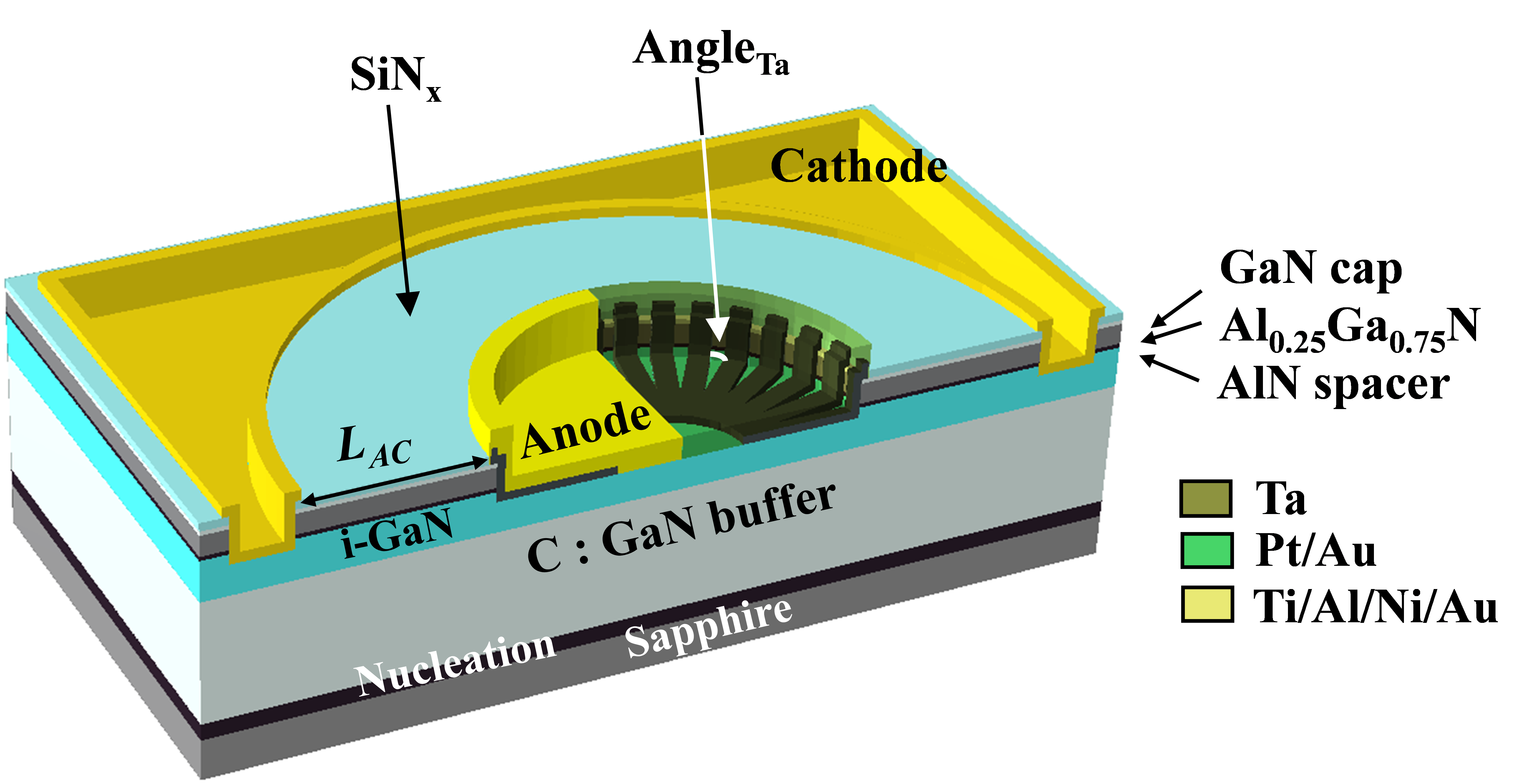
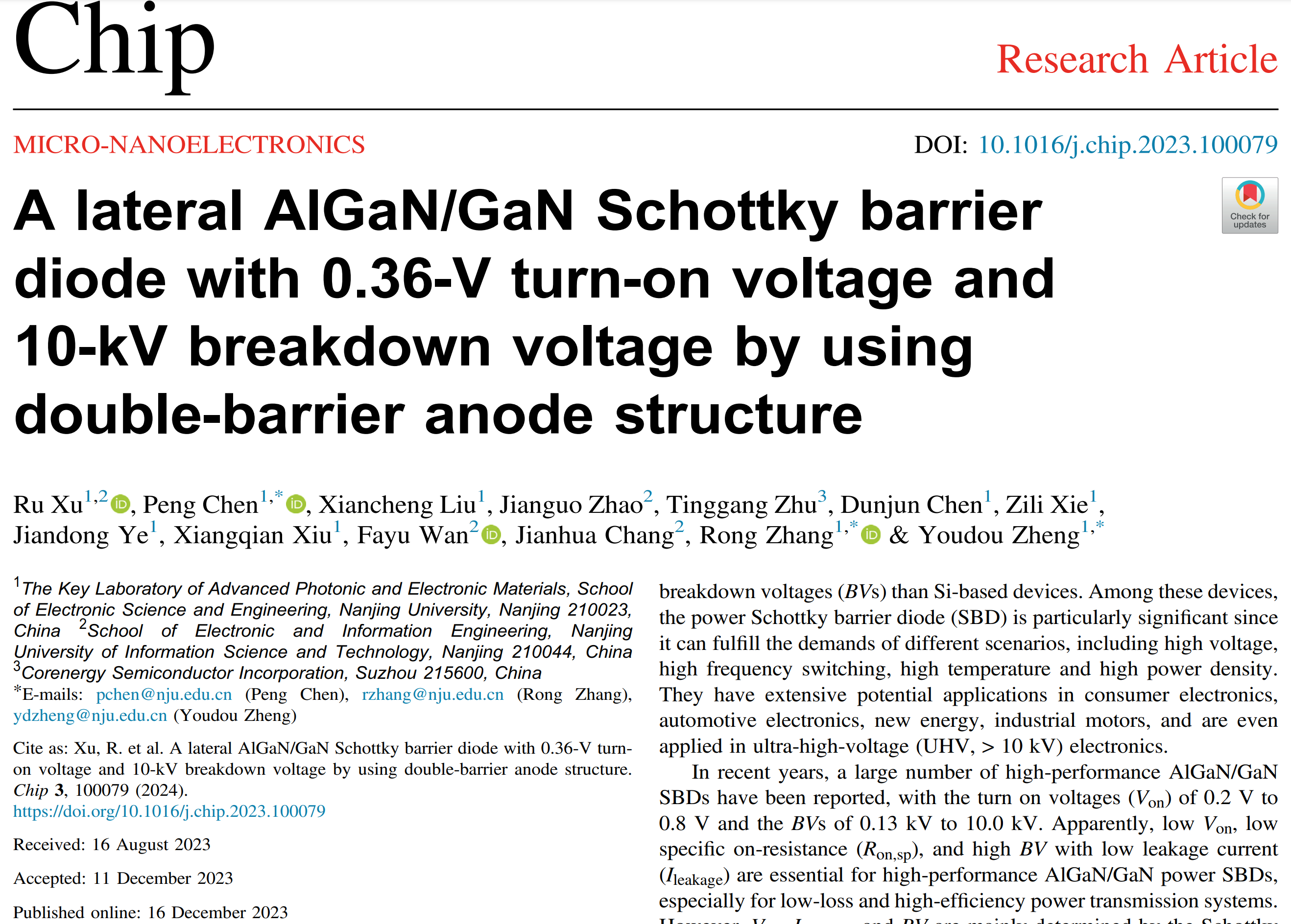
图1 | 具有齿状DBA结构的蓝宝石衬底AlGaN/GaN横向SBDs剖面示意图。
为了在保持肖特基电极高击穿电压的同时使用低功函数金属,需要一种新的电极结构设计。本工作从分析肖特基势垒的耗尽机制出发设计制备了双势垒阳极结构AlGaN/GaN SBD,研究者提出了由具有高功函数(铂Pt,5.65 eV)和低功函数(钽Ta,4.25 eV)组成的双势垒阳极(DBA)结构⁶。其创新地结合了这两种金属的特性,并将它们排列成交替的齿状图案,如图1所示。使用Silvaco软件研究了其降低器件开启电压的机制。研究发现器件在正向工作时的开启电压主要由低功函数的金属Ta决定,而器件在反向工作时的漏电和击穿主要由金属Pt决定,这种独特的性质主要是由肖特基结的势垒高度和耗尽层宽度呈正相关的关系决定。得益于蓝宝石衬底上高质量的碳掺杂GaN缓冲层的支持,最终制备的蓝宝石衬底AlGaN/GaN SBD的开启电压Von为0.36 V,有效降低了开启电压,比传统Pt电极结构器件的开启电压降低了约50%。为了评估器件性能的一致性,研究者对40个DBA SBD进行了测试并分析了结果,平均值为0.37 V,主导值为0.36 V,如图2所示。
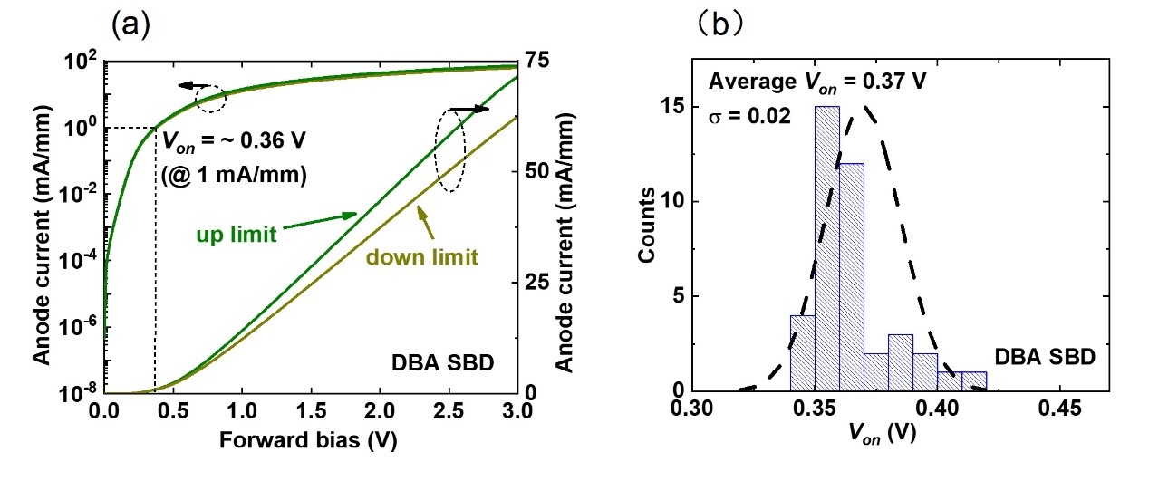
图2 | (a) 40个DBA SBD器件的正向I-V特性,(b) 开启电压分布。
对于反向I-V特性,DBA阳极器件的漏电流与Pt阳极相比有小幅升高,但Ta阳极器件相比,漏电流却下降了两个数量级,同时器件的击穿电压与Pt阳极保持了一致,均大于10 kV,超过Ta阳极器件的7 kV,如图3所示。器件特征导通电阻Ron,sp = 25.1 mΩ·cm²,Ileakage = 2.5×10⁻⁶ A/mm,功率品质因数(P-FOM)高达4.0 GW/cm²。
本工作SBD不仅在所有衬底上的所有GaN横向SBD中显示出较高的BV和P-FOM,而且同时实现了0.36 V的低开启电压,本工作GaN基横向SBD的BV和Von的对比基准曲线可参考论文图7¹。该项工作展示了GaN基功率电子器件的高性能潜力,以及其在低损耗和高效率的功率传输系统中的应用潜力。
图3 | DBA阳极器件、Pt阳极器件和Ta阳极器件的反向I-V特性。
A lateral AlGaN/GaN Schottky barrier diode with 0.36 V turn-on voltage and 10 kV breakdown voltage by using double barrier anode structure¹
III-V nitrides are typical wide-bandgap semiconductor materials. Among these, gallium nitride (GaN) is an excellent representative and finds extensive applications in the optoelectronics and power electronics fields. In particular, the AlGaN/GaN structure can generate a two-dimensional electron gas (2-DEG) with high electron concentration (~1×10¹³ cm⁻²) and high electron mobility (~2000 cm²/V·s). Combined with the high critical field (~3.3 MV/cm), power electronic devices based on AlGaN/GaN can have faster switching speeds, lower on-resistance, and higher breakdown voltages. They have a wide range of potential applications, including consumer electronics, automotive electronics, new energy, industrial motors, and even ultra-high voltage (UHV, >10 kV) electronic fields. Among these devices, power Schottky barrier diodes (SBDs) are particularly important and are one of the core components in power conversion systems. One of the key issues in developing GaN power SBDs is to create ultra-low loss/high-power devices, which involves effectively lowering the device's forward turn-on voltage (Von) and significantly increasing the breakdown voltage (BV) of the GaN SBD. Low Von / low specific on-resistance (Ron,sp) and high BV with low leakage current (Ileakage) are crucial for high-performance AlGaN/GaN power SBDs, especially for low loss and high-efficiency power transmission systems. In recent years, numerous high-performance AlGaN/GaN SBDs have been reported, with Von ranging from 0.2 V to 0.8 V and BV ranging from 0.13 kV to 10.0 kV. However, Von, Ileakage, and BV are mainly determined by the Schottky contacts, making it difficult to simultaneously improve all three parameters.
This research group has developed high-voltage GaN SBDs by studying the breakdown mechanism, leakage current transport mechanism, and depletion mechanism of GaN SBDs, focusing on reducing and optimizing the surface electric field during reverse bias of the device, anode trench preparation process, buffer layer and substrate material, and anode structure. Various terminal structures have been demonstrated to optimize the high-voltage SBD breakdown voltage, including our earlier reported 2.7-kV and 3.4-kV AlGaN/GaN SBDs with field plates²⁻³. According to the researcher’s previous studies, significant improvement in BV for AlGaN/GaN Schottky barrier diodes on Si substrates remains challenging. By using high-quality GaN material grown on sapphire substrates, they have reported high-performance AlGaN/GaN SBDs with BV exceeding 10 kV⁴⁻⁵.
Fig. 1 | Schematic diagram of lateral AlGaN/GaN SBDs with serrated DBA structure on sapphire substrate.
To maintain high breakdown voltage of the Schottky electrode while using low work function metal, a new electrode structure design is required. In this work, we have designed and prepared a double barrier anode structure AlGaN/GaN SBD, based on analyzing the depletion mechanism of the Schottky barrier. Researcher proposed a double barrier anode (DBA) structure composed of high work function (platinum Pt, 5.65 eV) and low work function (tantalum Ta, 4.25 eV) metals⁶. The researcher innovatively combined the characteristics of these two metals and arranged them in an alternating serrated pattern, as shown in Fig. 1. The mechanism for reducing the device's forward voltage was studied using Silvaco software. The study found that the device's forward voltage during normal operation is mainly determined by the low work function metal Ta, while the leakage and breakdown during reverse operation are mainly determined by the metal Pt. This unique property is primarily determined by the relationship between the barrier height and depletion layer width of the Schottky structure. Thanks to the support of high-quality carbon-doped GaN buffer layers on sapphire substrates, the final sapphire substrate AlGaN/GaN SBD has a forward voltage of 0.36 V, effectively lowering the forward voltage compared to traditional Pt electrode structure devices by approximately 50%. To evaluate the consistency of device performance, we tested and analyzed 40 DBA SBDs, with an average Von of 0.37 V and a dominant value of 0.36 V, as shown in Fig. 2.
Fig. 2 | (a) Forward I-V characteristics of 40 DBA SBD devices, (b) Turn-on voltage distribution.
For the reverse I-V characteristics, the leakage current of the DBA anode device is slightly higher compared to the Pt anode, but it is lower by two orders of magnitude compared to the Ta anode device. Meanwhile, the breakdown voltage of the device is consistent with the Pt anode, both exceeding 10 kV, surpassing the 7 kV of the Ta anode device, as shown in Fig. 3. The characteristic specific on-resistance Ron,sp of the device is 25.1 mΩ·cm², the Ileakage is 2.5×10⁻⁶ A/mm, and the P-FOM is as high as 4.0 GW/cm².
Fig. 3 | Reverse I-V characteristics of DBA anode device, Pt anode device and Ta anode device.
This work not only demonstrates higher BV and power P-FOM in all lateral GaN SBDs on all substrates, but also achieves a low forward voltage of 0.36 V at same time. The comparison reference curve of the BV and Von of the GaN-based lateral SBDs in this work may be seen in Fig. 7 of the original paper¹. This work showcases the high-performance potential of GaN-based power electronic devices and their potential applications in low-loss and high-efficiency power transmission systems.
参考文献:
1. Xu, R. et al. A lateral AlGaN/GaN Schottky barrier diode with 0.36-V turnon voltage and 10-kV breakdown voltage by using double-barrier anode structure. Chip 3, 100079 (2024).
2. Xu, R. et.al, 2.7-kV AlGaN/GaN Schottky barrier diode on silicon substrate with recessed-anode structure. Solid State Electron. 175, 107953 (2021).
3. Xu, R. et.al, 3.4-kV AlGaN/GaN Schottky barrier diode on silicon substrate with engineered anode structure. IEEE Electron Device Lett. 42, 208-211 (2021).
4. Xu, R. et.al. High power Figure-of-Merit, 10.6-kV AlGaN/GaN lateral Schottky barrier diode with single channel and sub-100-μm anode-to-cathode spacing. Preprint at https://doi.org/10.48550/arXiv.2108.06679 (2021).
5. Xu, R. et al. High power Figure-of-Merit, 10.6-kV AlGaN/GaN lateral Schottky barrier diode with single channel and sub-100-μm anode-to-cathode spacing. Small 18, 2270199 (2022).
6. Xu, R. et.al. A lateral AlGaN/GaN Schottky barrier diode with 0.36 V turn-on voltage and 10 kV breakdown voltage by using double barrier anode structure. Preprint at https://doi.org/10.48550/arXiv.2206.07881 (2022).
文章链接:
https://www.sciencedirect.com/science/article/pii/S2709472323000424
作者简介

徐儒,博士,南京大学博士后。博士毕业于南京大学,目前在南京信息工程大学电子与信息工程学院微电子系从事教学科研工作。主要从事氮化物半导体固体电子学与功率电子器件、氮化物半导体照明和光电探测器件研究,特别在优化GaN肖特基二极管(包括横向和准垂直结构)的器件结构及制备方面取得了一系列的开创性成果,目前在Small,EDL等期刊发表论文多篇,主持及参与科研项目4项。
Ru Xu, postdoctoral fellow at Nanjing University. Graduated from Nanjing University with a PhD degree, currently working in the Department of Microelectronics at the College of Electronic and Information Engineering, Nanjing University of Information Science & Technology. He engaged in teaching and research in the field of nitride semiconductor solid-state electronics and power electronic devices, solid state lighting, and photon detectors. Particularly, has made a series of pioneering achievements in optimizing the device structure of GaN Schottky diodes (including lateral and quasi-vertical structures). He published research papers in journals such as Small and EDL and has led and participated in four research projects.

陈鹏,南京大学电子与科学工程学院,教授,博导,长期从事三族氮化物材料与器件研究,取得了一批世界首创、国内领先的研究成果,是「江苏省高层次创新创业人才引进计划」获创新人才,江苏省有突出贡献中青年专家,国家「863」主题项目首席专家。主持多项国际合作项目、「863」项目、国家自然基金项目、江苏省重点研发项目等重大研究项目,申请国际/国家发明专利80余件,发表学术论文220余篇,SCI收录200余篇。
Peng Chen, professor and PhD supervisor at the School of Electronic Science and Engineering, Nanjing University, has long been engaged in research on III-nitride materials and devices, achieving a number of world-first and domestically leading research results. He is recognized as an Innovative Talent in “Jiangsu Province's High-level Innovation and Entrepreneurship Talent Introduction Program”, a Young and Middle-aged Expert with Outstanding Contributions in Jiangsu Province, and a Chief Scientist/Principal Investigator in national "863" projects. He has led several international collaboration projects, "863" projects, National Natural Science Foundation projects, Jiangsu Province key research and development projects, and other major research projects, with more than 80 international/national invention patent applications, and published over 220 research papers, with over 200 of them indexed in SCI.

张荣,中国科学院院士,厦门大学党委书记,厦门大学国家集成电路产教融合创新平台主任,厦门市未来显示技术研究院院长。他主要从事半导体光电子材料、器件和物理研究。在解决基础物理问题、攻克材料制备难题的基础上,他研制成功新型高性能紫外探测和固态光源器件,开拓高灵敏空天日盲紫外探测成像等应用领域,取得了系统性、创造性成就,产生重大社会经济效益。他的团队曾获国家技术发明二等奖、国家自然科学二等奖等多项奖项。
Rong Zhang, academician of the Chinese Academy of Sciences. He is mainly engaged in research on semiconductor optoelectronic materials, devices, and physics. Based on the resolution of basic physics problems and overcoming the difficulties in material preparation, he successfully developed new high-performance ultraviolet detection and solid-state light source devices and explored applications in areas such as high-sensitivity air and space-based ultraviolet detection and imaging. He has achieved systematic and innovative accomplishments and has produced significant social and economic benefits. His team has won numerous awards, including the National Technology Invention Second Prize and the National Natural Science Second Prize.
郑有炓,2003年当选为中国科学院院士。长期从事半导体异质结构材料与器件物理研究,近年主要致力于宽禁带半导体光电子材料与器件研究,取得大量国际领先研究成果。研究成果获得国家自然科学奖二等奖1项、国家技术发明奖三等奖1项、江苏省科技进步奖一等奖1项、江苏省人才培养教学成果一等奖1项、教育部自然科学一等奖和技术发明一等奖,以及其他省部级科技进步奖8项、国家863计划先进工作者一等奖。
Youliao Zheng, he was elected as an academician of the Chinese Academy of Sciences in 2003. He has long been engaged in the study of semiconductor heterostructure materials and device physics. In recent years, he has mainly devoted himself to the research of wide bandgap semiconductor optoelectronic materials and devices, achieving a large number of internationally leading research results. His research achievements have won one Second Prize of the National Natural Science Award, one Third Prize of the National Technical Invention Award, one First Prize of the Science and Technology Progress Award of Jiangsu Province, one First Prize of the Talent Training and Teaching Achievement Award of Jiangsu Province, a First Prize of Natural Science and Technical Invention awarded by the Ministry of Education, as well as 8 other provincial and ministerial-level Science and Technology Progress Awards and a First Prize for Advanced Workers in the national 863 Program.
关于Chip
Chip(ISSN:2772-2724,CN:31-2189/O4)是全球唯一聚焦芯片类研究的综合性国际期刊,已入选由中国科协、教育部、科技部、中科院等单位联合实施的「中国科技期刊卓越行动计划高起点新刊项目」,为科技部鼓励发表「三类高质量论文」期刊之一。
Chip期刊由上海交通大学出版,联合Elsevier集团全球发行,并与多家国内外知名学术组织展开合作,为学术会议提供高质量交流平台。
Chip秉承创刊理念: All About Chip,聚焦芯片,兼容并包,旨在发表与芯片相关的各科研领域尖端突破性成果,助力未来芯片科技发展。迄今为止,Chip已在其编委会汇集了来自14个国家的70名世界知名专家学者,其中包括多名中外院士及IEEE、ACM、Optica等知名国际学会终身会士(Fellow)。
Chip第三卷第一期已于2024年3月在爱思维尔Chip官网以金色开放获取形式(Gold Open Access)发布,欢迎访问阅读本期最新文章。
爱思唯尔Chip官网:
https://www.sciencedirect.com/journal/chip