Chip发表格勒诺布尔-阿尔卑斯大学A. G. M. Jansen团队最新成果
FUTURE远见| 2024-02-23
Future|远见
Future|远见future选编
近日,格勒诺布尔-阿尔卑斯大学A. G. M. Jansen团队最新研究成果以「Impedancemetry of multiplexed quantum devices using an on-chip cryogenic complementary metal-oxide-semiconductor active inductor」¹为题在Chip上发表研究论文,报道了测量低温谐振LC电路半导体量子位的量子电容的新方法。L. Le Guevel为文章第一作者,通讯作者为A. G. M. Jansen。本文为特刊(Cryogenic Chips)文章之一,此特刊为Chip发起的首个特刊。Chip是全球唯一聚焦芯片类研究的综合性国际期刊,是入选了国家高起点新刊计划的「三类高质量论文」期刊之一。
为了追求可扩展的量子处理器,人们已经投入了大量的精力来开发低温硬件,以控制和读出越来越多的量子位。本文提出了一种阻抗测量的新方法,适用于测量连接到谐振LC电路的半导体量子位的量子电容,谐振频率约为200 MHz。
行波分析的反射法中50 Ω阻抗匹配对实现最佳灵敏度起着至关重要的作用,与其不同,文章提出的阻抗测量方法依赖于通过局部施加电流和检测电压对谐振电路进行直接阻抗测量,其中包含要测量的电容。阻抗法与反射法的本质区别在于,阻抗法的灵敏度对谐振电路阻抗测量值的50 Ω阻抗匹配的依赖要小得多²⁻³。如图1所示,门控量子点器件的电容光谱检测结构内的电子量子态,包括第一占据的电子态。
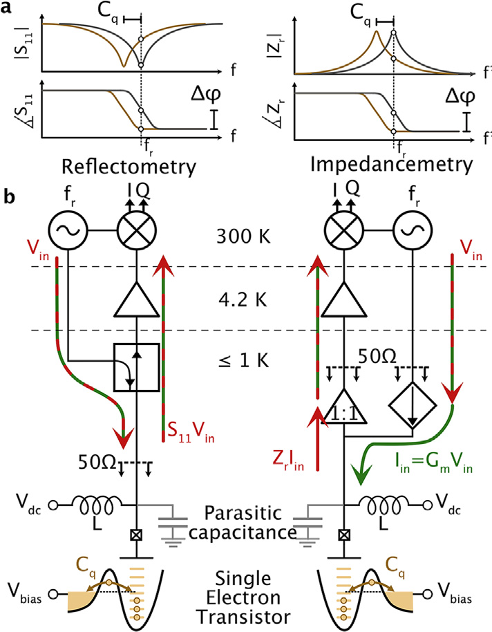
图1 | 测量量子电容的集成电路。
在没有低温模型的帮助下,电路的工作点需要从室温设置的偏置电压和电流开始实验确定。研究了n型金属氧化物半导体(MOS)阈值电压的升高(p型MOS同理),在4.2 K时通过施加1.2 V的反向电压来补偿。通过重复扫频监测阻抗,获得最佳低温共模电压 ���=0.48� ,直到出现��和��最低值的典型共振行为达到200 MHz。在��处,低温放大级的增益根据放大器和缓冲器的电流偏置进行了优化。阻抗测量在可调性和检测灵敏度方面的主要结果如图2所示。
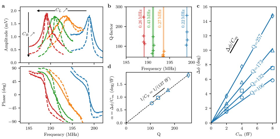
图2 | 谐振电路电容在4.2 K检测的表征。
通过校准的阻抗测量电路,研究者能够检测多路复用微型金属-氧化物-半导体场效应晶体管(MOSFETS)的门量子电容���,类似于使用互补金属-氧化物-半导体(CMOS)技术实现自旋量子位的电路⁴。图3给出栅极长度为120 nm,宽度为80 nm的器件M2的测量结果。实现的低温电路可以实现快速阻抗检测,测量电容分辨率低至10 aF,输入参考噪声为3.7 aF/ �� 。在4.2 K时,有源电感的功耗为120 μW,外加片上电流激励(0.15 μW)和电压放大(2.9 mW)的阻抗测量耗散。
测量量子器件的多路复用片外电容将有助于对许多量子器件进行系统筛选和测试,其实验装置比反射测量更简单。从长远来看,在低温条件下实现量身定制的高端模拟电子器件将改善并加速量子处理器的升级。
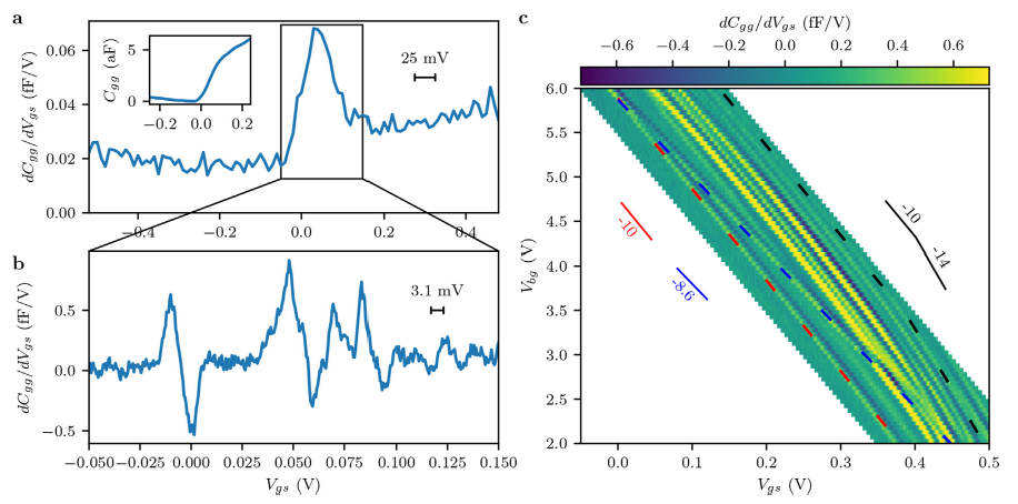
图3 | 沟道长度为120 nm,线宽为80 nm的集成MOSFET在4.2 K下的量子电容测量。
Impedancemetry of multiplexed quantum devices using an on-chip cryogenic complementary metal-oxide-semiconductor active inductor ¹
In the pursuit for scalable quantum processors, significant effort has been devoted to the development of cryogenic classical hardware for the control and readout of a growing number of qubits. In the current work, an alternative readout technique called impedancemetry was adopted for measuring the impedance of the LC tank at resonance, which in our case is around 200 MHz.
Unlike the reflectometry method based on traveling wave analysis where 50 Ω impedance matching plays a crucial role in achieving the optimal sensitivity, the proposed impedancemetry method relies on the direct impedance measurement of a resonant circuit which contains the capacitance to be measured through the locally applied currents and detected voltages. As an essential difference with reflectometry, the sensitivity of impedancemetry depends much less on the 50 Ω matching criterion for the measured value of the impedance of the resonant circuit²⁻³. As shown in Fig. 1, capacitive spectroscopy of gate-controlled quantum-dot devices allow the detection of electronic quantum states within the structure, including the firstly occupied electron states.
Fig. 1 | Integration of measuring circuitry for readout of quantum capacitance.
Without the assistance of low-temperature models, the operating point of the circuit needs to be determined experimentally starting from room-temperature settings of bias voltages and currents. The increase in threshold voltage of n-type metal-oxide-semiconductor (resp. p-type metal-oxide-semiconductor) transistors at 4.2 K is compensated by applying a back-gate voltage of 1.2 V (resp. −2 V). The optimal cryogenic. common-mode voltage ���=0.48� was obtained while monitoring the tank impedance via repeated frequency sweeps until a typical resonance behavior up to 200 MHz emerges for the lowest values of �� and �� . The gain of the low-temperature amplification stage at �� is optimized with respect to the current bias of amplifier and buffer. The main results of the impedancemetry with respect to tunability and detection sensitivity are shown in Fig. 2.
Fig. 2 | Characterization of the resonant circuit at 4.2 K for capacitance detection.
With the calibrated impedancemetry circuit, we are able to detect the gate quantum capacitance ��� of the multiplexed tiny metal–oxide–semiconductor field-effect transistor (MOSFETs) similar to the ones used to implement spin qubits with technology⁴. Complementary metal-mxide-semiconductor (CMOS) Measurements will be presented for M2 with a gate length of 120 nm and a gate width of 80 nm in Fig. 3. The realized cryogenic circuit allows fast impedance detection with a measured capacitance resolution down to 10 aF and an input-referred noise of 3.7 aF/ �� . At 4.2 K, the power consumption of the active inductor amounts to 120 μW, with an additional dissipation for on-chip current excitation (0.15 μW) and voltage amplification (2.9 mW) of the impedance measurement.
Measuring multiplexed out-of-chip capacitances of quantum devices will be also promising for the systematic screening and testing of many quantum devices with a simpler experimental setup than reflectometry. In the long run, the realization of tailored high-end analog electronics at cryogenic temperatures will improve and accelerate the up-scaling of quantum processors.
Fig. 3 | Quantum capacitance measurement of an integrated MOSFET with a channel length of 120 nm and a width of 80 nm at 4.2 K.
参考文献:
1. Guevel, L. Le et al. Impedancemetry of multiplexed quantum devices using an on-chip cryogenic complementary metal-oxide-semiconductor active inductor. Chip 2, 100068 (2023).
2. Shor, P. W. Polynomial-time algorithms for prime factorization and discrete logarithms on a quantum computer. SIAM J. Comput. 26, 1484e1509 (1997).
3. Grover, L. K. Quantum mechanics helps in searching for a needle in a haystack. Phys. Rev. Lett. 79, 325 (1997).
4. Maurand, R. et al. A CMOS silicon spin qubit. Nat. Commun. 7, 13575 (2016).
论文链接:
https://www.sciencedirect.com/science/article/pii/S270947232300031X
作者简介

L. Le Guevel,法国科学家,从事量子计算,量子控制和量子技术的跨学科研究。主要专注于设计和演示替代架构,权衡控制电子和量子处理器设计,这可能使大规模量子计算成为现实。自2017年以来,一直致力于低温集成电路设计组和量子物理团队的联合研究项目。
L. Le Guevel,a French-born research scientist, who recently relocated to the USA, with a strong affinity for interdisciplinary research in quantum computing, quantum control, and quantum technologies. He mainly focuses on designing and demonstrating alternative architectures, trading off control electronics and quantum processor design, that could make large-scale quantum computation a reality. Since 2017, He has been contributing to joint research projects between cryogenic integrated circuit design groups and quantum physics teams.
关于Chip
Chip(ISSN:2772-2724,CN:31-2189/O4)是全球唯一聚焦芯片类研究的综合性国际期刊,已入选由中国科协、教育部、科技部、中科院等单位联合实施的「中国科技期刊卓越行动计划高起点新刊项目」,为科技部鼓励发表「三类高质量论文」期刊之一。
Chip期刊由上海交通大学出版,联合Elsevier集团全球发行,并与多家国内外知名学术组织展开合作,为学术会议提供高质量交流平台。
Chip秉承创刊理念: All About Chip,聚焦芯片,兼容并包,旨在发表与芯片相关的各科研领域尖端突破性成果,助力未来芯片科技发展。迄今为止,Chip已在其编委会汇集了来自14个国家的70名世界知名专家学者,其中包括多名中外院士及IEEE、ACM、Optica等知名国际学会终身会士(Fellow)。
Chip第二卷第四期已于2023年12月在爱思维尔Chip官网以金色开放获取形式(Gold Open Access)发布,欢迎访问阅读本期最新文章。
爱思唯尔Chip官网:
https://www.sciencedirect.com/journal/chip